0去购物车结算
购物车中还没有商品,赶紧选购吧!
当前位置: 图书分类 > 工程技术 > 水利工程 > 现代VLSI电路设计—芯片系统设计 第三版 英文影印版

相同语种的商品

现代VLSI电路设计—芯片系统设计 第三版 英文影印版


联系编辑
 
标题:
 
内容:
 
联系方式:
 
  
现代VLSI电路设计—芯片系统设计 第三版 英文影印版
  • 书号:7030111494
    作者:(美)沃 尔夫(Wolf,W.)著
  • 外文书名:
  • 装帧:平装
    开本:16开
  • 页数:640
    字数:919000
    语种:英文
  • 出版社:科学出版社
    出版时间:2003-03-23
  • 所属分类:TN4 微电子学、集成电路(IC)
  • 定价: ¥48.00元
    售价: ¥37.92元
  • 图书介质:

  • 购买数量: 件  缺货,请选择其他介质图书!
  • 商品总价:

相同系列
全选

内容介绍

用户评论

全部咨询

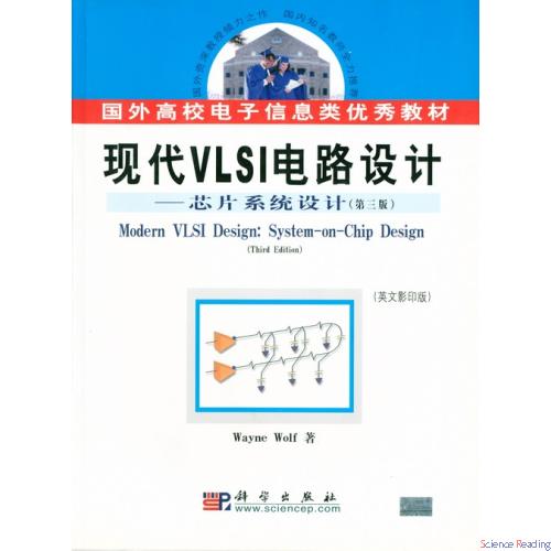
本书为国外高校电子信息类优秀教材(英文影印版)之一。
本书介绍了完整的VLSI设计过程——从物理设计到系统结构,为VLSI系统设计者提供了这一过程的全面介绍,同时对硬件描述语言VHDL进行了深入的讨论。
本书可作为电子工程、计算机专业本科生教材,也可作为相关领域工程技术人员的参考书。
  • 暂时还没有任何用户评论
总计 0 个记录,共 1 页。 第一页 上一页 下一页 最末页

全部咨询(共0条问答)

  • 暂时还没有任何用户咨询内容
总计 0 个记录,共 1 页。 第一页 上一页 下一页 最末页
用户名: 匿名用户
E-mail:
咨询内容:

目录

  • Preface to the Third Edition
    Preface to the Second Edition
    Preface
    1 Digital Systems and VLSI
    1.1 Why Design Integrated Circuits?
    1.2 Integrated Circuit Manufacturing
    1.3 CMOS Technology
    1.4 Integrated Circuit Design Techniques
    1.5 A Look into the Future
    1.6 Summary
    1.7 References
    1.8 Problems
    2 Transistors and Layout
    2.1 Introduction
    2.2 Fabrication Processes
    2.3 Transistors
    2.4 Wires and Vias
    2.5 Design Rules
    2.6 Layout Design and Tools
    2.7 References
    2.8 Problems
    3 Logic Gates
    3.1 Introduction
    3.2 Combinational Logic Functions
    3.3 Static Complementary Gates
    3.4 Switch Logic
    3.5 Alternative Gate Circuits
    3.6 Low-Power Gates
    3.7 Delay Through Resistive Interconnect
    3.8 Delay Through Inductive Interconnect
    3.9 References
    3.10 Problems
    4 Combinational Logic Networks
    4.1 Introduction
    4.2 Standard Cell-Based Layout
    4.3 Simulation
    4.4 Combinational Network Delay
    4.5 Logic and Interconnect Design
    4.6 Pwer Optimization
    4.7 Switch Logic Networks
    4.8 Combinational Logic Testing
    4.9 References
    4.10 Problems
    5 Seqential Machines
    5.1 Introduction
    5.2 Latches and Flip-Flops
    5.3 Sequential Systems and Clocking Disciplines
    5.4 Sequential System Design
    5.5 Power Optimaization
    5.6 Design Validation
    5.7 Sequential Testing
    5.8 References
    5.9 Problems
    6 Subsystem Design
    6.1 Introduction
    6.2 Subsystem Design Principles
    6.3 Combinational Shifers
    6.4 Adders
    6.5 ALUs
    6.6 Multipliers
    6.7 High-Density Memory
    6.8 Field-Programmable Gate Arrays
    6.9 Programmable Logic Arrays
    6.10 Refernces
    6.11 Problems
    7 Floorplanning
    7.1 Introduction
    7.2 Floorplanning Methods
    7.3 Off-Chip Connections
    7.4 References
    7.5 Problems
    8 Architecture Design
    8.1 Introduction
    8.2 Hardware Description Languages
    8.3 Register-Transfer Design
    8.4 High-Level Synchesis
    8.5 Architectures for Low Power
    8.6 Systems-on-Chips and Embedded CPUs
    8.7 Architecture Testing
    8.8 References
    8.9 Problems
    9 Chip Design
    9.1 Introduction
    9.2 Design Methodologies
    9.3 Kitchen Timer Chip
    9.4 Microprocessor Data Path
    9.5 References
    9.6 Problems
    10 CAD Systems and Algorithms
    10.1 Introduction
    10.2 CAD Systems
    10.3 Switch-Level Simulation
    10.4 Layout Synthesis
    10.5 Layout Analysis
    10.6 Timing Analysis and Optimization
    10.7 Logic Synthesis
    10.8 Test Generation
    10.9 Sequential Machine Optimizations
    10.10 Scheduling and Binding
    10.11 Hardware/Software Co-Design
    10.12 References
    10.13 Problems
    A Chip Designer's Lexicon
    B Chip Design Projects
    B.1 Class Project Ideas
    B.2 Project Proposal and Specification
    B.3 Design Plan
    B.4 Design Checkpoints and Specification
    C Kitchen Timer Model
    C.1 Hardware Modeling in C
    Index
帮助中心
公司简介
联系我们
常见问题
新手上路
发票制度
积分说明
购物指南
配送方式
配送时间及费用
配送查询说明
配送范围
快递查询
售后服务
退换货说明
退换货流程
投诉或建议
版权声明
经营资质
营业执照
出版社经营许可证